What does the transition to glass and ceramic substrates truly demand?
TGV (Through-Glass Via) and TCV (Through-Ceramic Via) technologies are rapidly replacing organic substrates in following applications:
- High-speed optical/electrical interconnects
- 5G/6G and millimeter-wave RF modules
- High-bandwidth AI modules
- Miniaturized medical sensors
- Automotive-grade electronics requiring extreme reliability
Advantages:
- Ultra-low dielectric loss compared with organic substrates
- CTE well-matched to silicon
- Excellent insulation and thermal stability
- Support for finer pitch and higher-density 3D vertical interconnects
However, the true challenge is creating reliable, continuous, low-resistance metal pathways through these materials.
For high-aspect-ratio vias (10:1 to 15:1), any failure in metallization means the entire package is scrap. This remains one of the industry’s biggest bottlenecks—and exactly where Huicheng Vacuum’s technology enters as a decisive enabler.
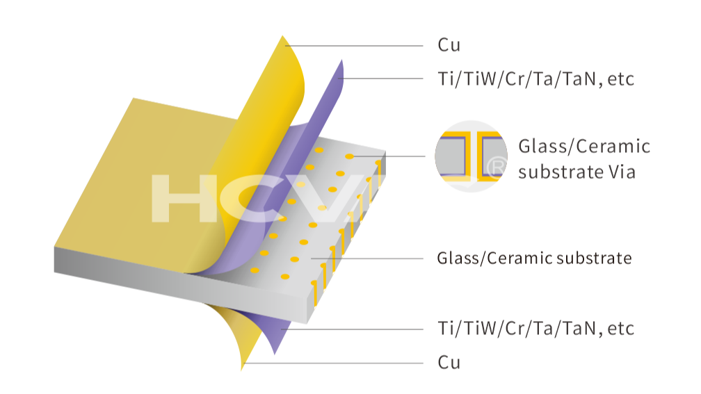
TGV Structures and Via-Fill Techniques: The Engineering Science Behind Reliable Metallization
TGV Geometries
Depending on how the vias are formed—typically through laser drilling or wet/dry etching—TGVs generally fall into four categories:
- Blind vias
- Through vias
- X-shaped vias
- V-shaped vias
Compared with TSV, TGV usually features larger diameters and full-depth vias, which increase plating time and overall process cost.
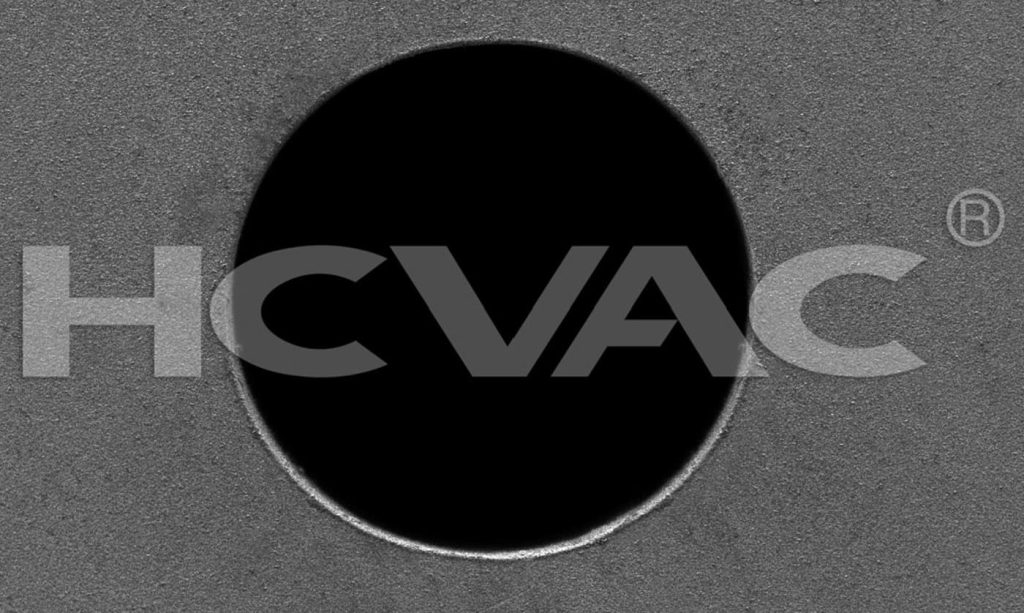
Because glass has an extremely smooth surface, common metals such as copper tend to peel or curl, leading to delamination between the substrate and the metallization layer.
Via geometry plays a critical role in determining electrical performance, long-term reliability, fabrication cost, and overall process complexity.
Leveraging their inherent brittleness, excellent insulation, and superior high-frequency characteristics, glass substrates are increasingly adopted in 2.5D/3D IC packaging, RF components, MEMS sensors, and advanced display modules.
TGV Via-Fill Technologies
Achieving void-free and seam-free filling requires different approaches depending on the via structure.
Bottom-Up Filling (for blind and V-shaped vias)
- Suppressor additives adsorb near the via opening to slow deposition at the top
- Accelerators concentrate at the via bottom to promote faster copper growth
- Copper grows from the bottom upward, preventing voids and seam formation
Butterfly Filling (BFT, for straight through-vias)
- Growth starts near the center and progresses toward both ends, avoiding premature closure
- Improved electrolyte flow inside the via enhances mass transport
- Dual-direction plating increases overall fill rate
- Geometry-driven and hydrodynamic effects maintain stable filling even when conventional blind-via chemistries fail
HCVAC’s Metallization Platform Purpose-Built for High-Aspect-Ratio TGV/TCV Vias
TGV/TCV metallization imposes far more demanding requirements than conventional PVD systems, including:
- Higher plasma density
- Extremely uniform ion distribution
- Increased ionization efficiency
- Precise substrate bias control
- Stable, long-duration deposition for complex via structures
TGV/TCV metallization imposes far more demanding requirements than conventional PVD systems, including:
- Higher plasma density
- Extremely uniform ion distribution
- Increased ionization efficiency
- Precise substrate bias control
- Stable, long-duration deposition for complex via structures
Core Capabilities
- Reliable metallization inside high-aspect-ratio vias (up to 15:1)
- Load-locked magnetron sputtering system
- RF, DC, and HiPIMS high-power pulsed sputtering for superior step coverage
- Combined pulsed-bias modes ensuring continuous bottom coverage, low via resistance, and zero shadowing
- Surface metallization and RDL (Redistribution Layer) formation
- Seed-layer deposition for fine-pitch routing (Ti/Cu and other stacks)
- ≤ ±3% thickness uniformity across large-format glass panels
- Full support for high-frequency interconnects, OEIC (optical-electronic co-packaging), and MEMS integration
- Multi-target, multi-layer sputtering for complex film stacks
- Simultaneous sputtering of Ti, Cu, Al, ITO, and other materials
- Enables metal layers, resistor films, diffusion barriers, and adhesion layers
- Films optimized for high hardness, low stress, corrosion resistance, and excellent electrical performance
TGV PVD Seed Layer AR 15:1
Process Capability: Engineered for High-Volume Manufacturing
Item | Specification |
Wafer Size | 6–8 inches |
Glass Substrates | G1.0–G5.0 (100 × 100 mm to 1100 × 1300 mm) |
Via Dimensions | Diameter 20–300 μm, Depth 100–1500 μm |
Aspect Ratio | Up to 15:1, full-coverage metallization |
Film Uniformity | ≤ ±3% |
Warp/Flatness Control | Low warpage, high planarity |
Production Throughput | Multi-cassette automated loading/unloading with carrier-locked transfer |
Process Data | Automated logging with full quality traceability |
This means HCVAC is equipped not only for lab-scale demonstrations, but truly for volume production.
TGV/TCV Metallization: A Strategic Process for Advanced Packaging
As Chiplet architectures become the mainstream for AI servers, consumer electronics, and automotive systems, the demand for high-bandwidth, low-latency vertical interconnects is reaching unprecedented levels.
TGV/TCV metallization is emerging as a foundational enabling technology for:
- GPU and AI accelerator modules
- Co-Packaged Optics (CPO)
- High-frequency, high-speed networking ICs
- Mini/Micro-LED driver circuits
- MEMS and sensor arrays
- Miniaturized medical devices
Companies capable of high-aspect-ratio via metallization will hold the core advantage in the next era of advanced packaging.
In China, only a handful of companies can support large-format glass panels, 15:1 aspect-ratio vias, ≤±3% uniformity, and stable high-volume manufacturing—and HCVAC is among the key leaders in this field.
Conclusion: From Equipment Localization to Breakthroughs in Advanced Packaging Infrastructure
Over the past decade, competition in China’s thin-film equipment market centered on PVD stability and target utilization.
Today, the benchmark has shifted: whether equipment can fully support the technology development of Chiplet, 3D integration, and optoelectronic packaging.
HCVAC’s TGV/TCV metallization platforms bridge the full gap from fundamental research to high-volume manufacturing:
- From usable to production-grade
- From lab validation to high-volume manufacturing
- From single layers to engineered multilayer metal stacks
- From basic deposition to full-flow support for advanced packaging
This is more than an equipment upgrade—it represents a step-change in the capability of the entire semiconductor packaging ecosystem.