TGV – A Core Interconnect Solution for High-Performance Packaging
In multi-die integration and system-level packaging, technologies such as RDL, EMIB, CoWoS, and FOPLP have all advanced. But for larger package sizes and higher interconnect density, silicon interposers still face major limits: high cost and serious warpage risks.
By contrast, TGV glass substrates are becoming a key focus thanks to their core strengths:
Low dielectric loss: 1–2 dB lower insertion loss than silicon at 10 GHz, cutting energy loss in high-speed transmission.
High resistivity and low crosstalk: noise coupling between vias is reduced by more than 50%, ensuring signal integrity.
Excellent dimensional stability: CTE controlled at 3–9 ppm/K, reducing warpage risk.
High-speed interconnects: supports data rates above 70 Gb/s, meeting bandwidth needs for AI training and inference.Line width scaling potential:
RDL traces can shrink to ≤2 μm, enabling ultra-high-density interconnects.
In other words, TGV is not just a material replacement — it is a real upgrade in the interconnect paradigm.
TGV from a Customer Value Perspective
For end customers, the value of TGV glass substrates goes beyond “higher performance.” The real gains come from system-level benefits:
High reliability: reduce stress on micro-bump solder joints, extending product lifetime.
Scalability: supports panel-level manufacturing, where large panels greatly boost capacity and integration efficiency.
System integration: allows passive components to be embedded in the glass substrate, enabling a more compact package design.
Wide applications: whether in advanced AI chip packaging, optoelectronics, or MiniLED backlight and display modules, TGV provides stable high-density interconnects and thermal support.
This means that when customers deploy GPU training clusters, AI accelerator cards, or HPC systems, TGV packaging delivers higher compute density, lower energy use, and better return on investment.
Market Outlook – Entering a New Multi-Billion-Dollar Track
According to industry forecasts, the global glass substrate market could reach tens of billions of dollars by 2030. TGV adoption in AI servers, GPUs, and advanced packaging will rise quickly:
Within 3 years: TGV penetration in AI packaging may exceed 30%.
Within 5 years: penetration is expected to surpass 50%, making it a mainstream path for advanced packaging.
At the same time, industry giants such as Samsung, TSMC, Intel, and NVIDIA are all ramping up their investments in glass substrates. This is driving upgrades across materials, equipment, and processes throughout the supply chain.
It is clear that within the next five years, TGV will become one of the fastest-growing technologies in global advanced packaging.
HCVAC’s TGV Solution
As a leading company in vacuum coating and advanced packaging equipment, Guangdong Huicheng Vacuum Technology Co., Ltd. (HCVAC) has built a complete TGV solution based on years of expertise.
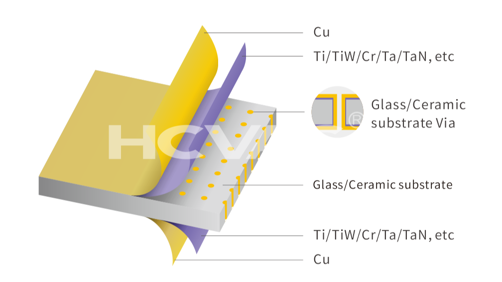
cross-section of a high-aspect-ratio TGV seed layer.
Comprehensive coverage: supports 6–8 inch wafers and G1.0 to G5.0 glass substrates (100×100 mm to 1100×1300 mm), with aspect ratios reach up to 15:1. It supports multiple target materials such as Ti and Cu, fully meeting the requirements of TGV/TCV metal seed layer deposition.
Reliable metallization: optimized electroplating and seed layer deposition ensure uniform via filling, reducing voids and cracks.
Large glass panel capability: supports panel-level packaging production such as FOPLP.
HiPIMS and sputtering process: high-power impulse magnetron sputtering (HiPIMS) achieves high ionization and dense films, solving the uneven coating problem of traditional via deposition and providing reliable support for packaging.
With these technologies, HCVAC not only provides a solid process foundation for high-performance packaging, but also shows strong application potential in AI chips, GPUs, optoelectronic devices, and MiniLED.
Conclusion
TGV technology is becoming a key pillar for AI computing upgrades and high-performance packaging. As Moore’s Law nears its limits and heterogeneous integration accelerates, TGV offers customers system-level solutions with higher reliability, larger package sizes, and lower energy use.
Leveraging its mature vacuum coating machine and breakthroughs in HiPIMS and magnetron sputtering, HCVAC is helping industry customers overcome bandwidth bottlenecks, improve computing efficiency, and drive leapfrog progress for China’s advanced packaging industry in global competition.
Looking ahead, as AI and HPC continue to demand higher interconnect performance, the market space for TGV will expand rapidly, making it an indispensable part of the packaging value chain.