Equipment

Application

Technology

Information

Let's Get in Touch!

Contact Form-产品详情页
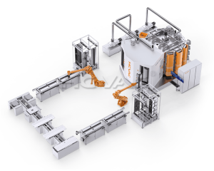
Vacuum Coating Machine Solution for AI Computing
Designed for semiconductor and photonics manufacturing across CPO, RDL, TGV/TSV, FOPLP, and other critical processes.
Contact Us

Supporting Advanced Semiconductor & Photonics Manufacturing

As AI computing continues to drive unprecedented demand for higher bandwidth, faster data transmission, and greater integration, advanced packaging and photonics manufacturing have become the foundation of next-generation AI infrastructure. 

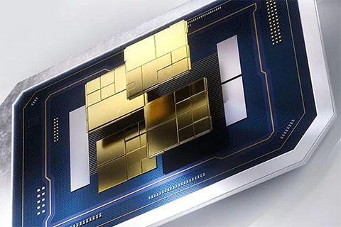
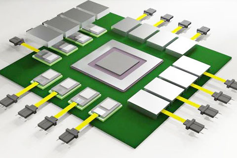
Our vacuum coating solutions support critical processes including Co-Packaged Optics (CPO), Redistribution Layer (RDL), Through-Glass/Through-Silicon Vias (TGV/TSV) and Fan-Out Panel Level Packaging (FOPLP), delivering high-performance thin films with exceptional uniformity, precision, and production stability.

How Vacuum Coating Enables Critical AI Chip Manufacturing Processes

CPO

Co-Packaged Optics (CPO)

High-precision thin-film deposition enables the fabrication of optical components, reflective coatings, and metallization layers for co-packaged optics, helping reduce optical loss, improve coupling efficiency, and support ultra-high-speed optical interconnections for AI data centers.

Redistribution Layer (RDL)

Uniform seed layer and metallization deposition provide reliable signal routing between chips and substrates, supporting fine-line redistribution with excellent adhesion, low electrical resistance, and consistent process stability.

RDL
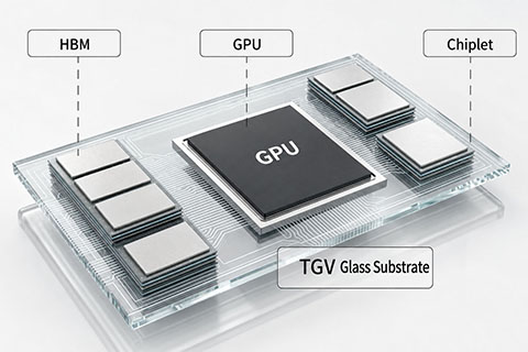
TGV Through Glass Vias

Through-Glass / Through-Silicon Via (TGV/TSV)

Precision sputtering technology forms conformal seed and conductive layers inside high-aspect-ratio vias, enabling reliable vertical electrical interconnections with excellent coverage, conductivity, and long-term process repeatability.

Fan-Out Panel-Level Packaging (FOPLP)

Deposit Cu seed layers, barrier layers, and adhesion films prior to electroplating, providing uniform metallization across large-format panels. This enables fine-line redistribution, high-yield copper plating, and reliable interconnect formation for high-density AI packaging.

FOPLP

Recommended Vacuum Coating Systems

Accelerate Your AI Manufacturing Innovation

Whether you're evaluating a new production line, optimizing an existing process, or developing next-generation packaging technologies, our engineering team is ready to support your project from concept to production.

Your Questions, Answered

What vacuum process technologies are used in advanced packaging manufacturing?

Advanced AI packaging manufacturing relies on multiple vacuum process technologies rather than a single deposition method. Depending on the application, these may include plasma surface treatment, soft etching, magnetron sputtering (PVD), PECVD, and ALD/PEALD to form conductive, dielectric, barrier, passivation, and functional thin films.

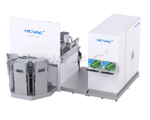
HCVAC's Cluster Deposition Platform integrates these core process modules into a single vacuum environment, enabling flexible multi-process manufacturing for CPO, RDL, TGV, FOPLP.

Which thin-film materials are used for AI packaging?

Advanced AI packaging relies on a variety of thin-film materials to build reliable electrical interconnections and functional structures. Common materials include copper (Cu) for seed layers and interconnects, titanium (Ti) and titanium tungsten (TiW) for adhesion and barrier layers, tantalum (Ta) and tantalum nitride (TaN) for diffusion barriers, and dielectric films such as silicon dioxide (SiO₂) and silicon nitride (SiN) for insulation and passivation.

HCVAC's vacuum deposition systems support a wide range of metallic and dielectric thin-film materials for advanced packaging manufacturing.

Send your inquiry now

We're pleased to solve your challenges and help you achieve your goals with our expertise

Contact with whatsapp button

Let's Get in Touch!

Contact Form-产品详情页