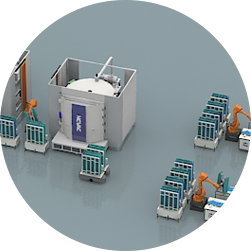
High precision Magnetron Sputtering Optical Coating Machine
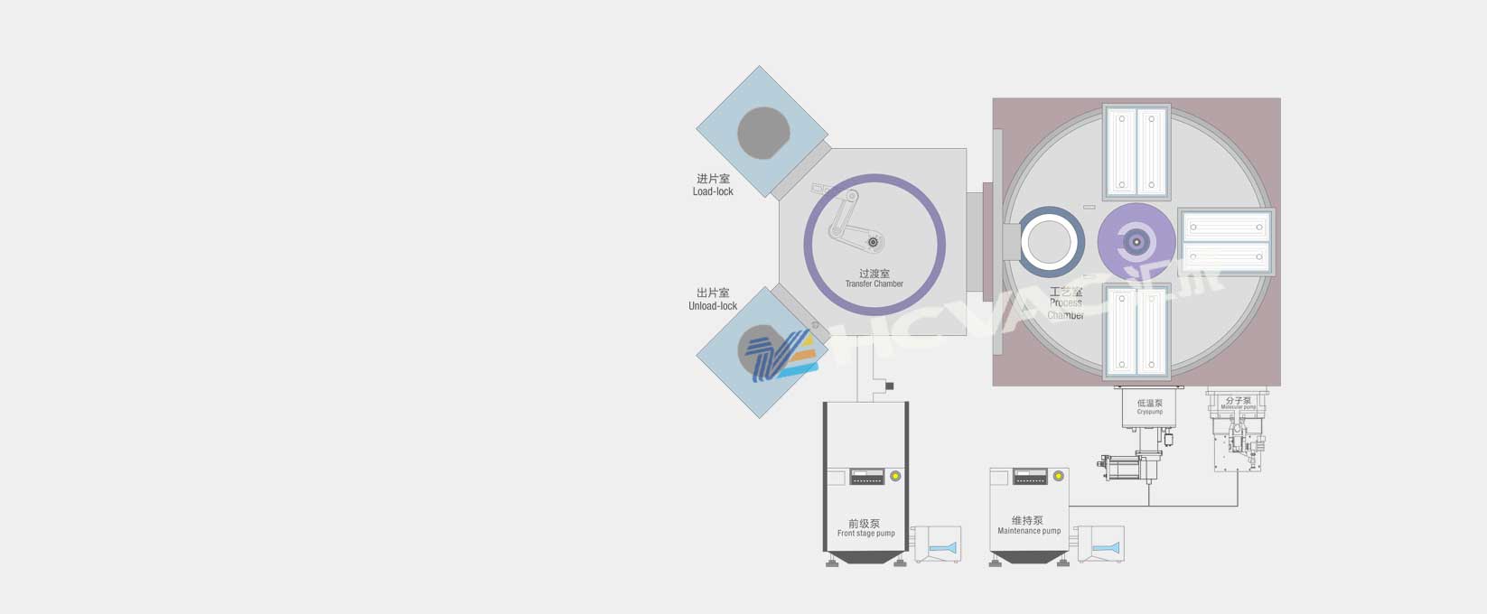
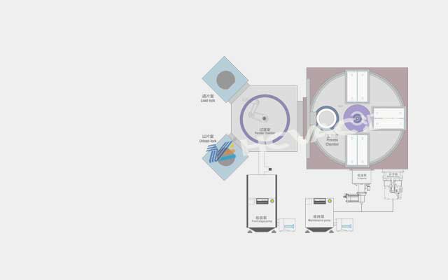
The modular design of the equipment can be combined with plasma clean unit, magnetron sputtering unit, plasma enhanced chemical reaction (PECVD) unit, atomic layer deposition (ALD) unit and plasma chemical reaction etching (RIE) unit to expand the cluster micro nano machining center, covering the substrate cleaning and thin film deposition (including ultra-thin film) of semiconductor micro nano structure processing Film etching and patterning. It can meet the strict film deposition uniformity specification, reduce the defects of high stress film to the greatest extent, increase the output and reduce the cost.
ICP Assisted Magnetron sputtering is used to process all kinds of band-pass films and cut-off films with low absorption and low stress, such as face ID, mid and far infrared high transmittance films; magnetron sputtering is used to process all kinds of metals such as Cu, Al, Cr, Au, Ag, SUS, etc.